 by Tega Akuruli
PCB Hardware: The Backbone of Modern Electronics
Why PCB Design Is the Backbone of Modern Electronics
Modern electronics are celebrated for their software: kudos go to artificial intelligence, apps, and smart automation. However, none of these innovations would work without the Printed Circuit Boards underneath: the invisible yet critical foundation that connects, powers, and stabilizes every electronic device.
PCBs offer:
- Mechanical support: Holding components in precise positions
- Electrical connectivity: Allowing signals to flow reliably between components
- Thermal Management: To conduct and dissipate heat before damage occurs.
- Signal integrity: Maintaining performance at high speeds
- Electromagnetic shielding: Prevention of noise interference
In other words, PCBs are the physical highways that make digital electronics possible. While software can be updated or patched, hardware is governed only by the laws of physics.
Understanding the basics of the design of a PCB is important not only for engineers but also for any person trying to understand how modern devices work.
This guide will take a closer look at the world of design, from basic components to high-speed design, thermal management, EMI/EMC challenges, HDI technology, flexible PCBs, manufacturing constraints, AI-assisted design tools, and future trends.
Understanding the Basics of PCBs
What a PCB Really Is
A Printed Circuit Board is not just a green flat board with copper traces. It is a carefully engineered platform for electronics, designed to perform multiple critical functions:
- Mechanical support: It holds all components such as ICs, resistors, capacitors, and connectors.
- Electrical connectivity: Copper traces form exact paths for electrical signals.
- Power delivery: It provides stable voltage and current to every component.
- Thermal management: Conducts heat away from sensitive components.
- Noise mitigation: Prevents unwanted interference between signals.
It’s like a little city-roads (traces) interconnect buildings (components); the power stations or planes dispense electricity; the heat management systems, copper pours, and VIAs keep everything cool, while the traffic rules, impedance, differential pairs, and shielding avoid collisions.
Evolution of the technology of PCBs
The technology of PCBs has evolved from humble beginnings to extremely complicated modern systems:
- Single-layer boards: The earliest PCBs with basic wiring.
- Double-layer boards: VIAs were introduced, allowing top and bottom layers to connect, making more complex circuits.
- Multi-layer HDI boards: High-Density Interconnect boards featuring multiple layers with microvias, enabling compact devices.
- Flexible and rigid-flex PCBs: These allow boards to fold or conform to curved shapes; highly important in wearables, medical devices, and aerospace.
- High-speed digital and RF PCBs: Which are designed for operations at GHz frequencies, featuring precise impedance control.
Each evolution allowed electronics to become smaller, faster, and more reliable.
The Anatomy of a PCB
Layers and Their Functions
- Substrate (FR-4, Rogers, or Polyimide): Provides mechanical support and dielectric insulation. The thermal stability, thickness, and dielectric constant will determine the speed of the signals and the EMI behavior.
- Copper Layers: These provide a path for signals and power. High-performance boards can have 8–32 layers. The layer count impacts signal integrity, EMI control, and manufacturing complexity.
- Solder Mask: A protective layer, preventing copper corrosion and shorts during soldering.
- Silkscreen: Printed markings for components, orientation, and assembly instructions.
- Planes (Power and Ground): Large areas of copper that provide stabilizing voltages, reduce EMI, and help with thermal distribution.
Main PCB Components
- Traces: Copper paths that connect components. The width, thickness, and length determine resistance, inductance, and impedance.
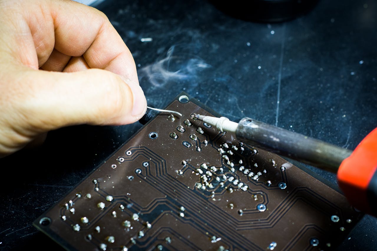
- Pads: They are exposed copper areas on a circuit board where components are soldered to create an electrical connection. They act as the physical and electrical link between a component’s pin and the board’s traces.
- VIAs: Is the electrical connection, typically a small drilled and plated hole, that passes through two or more layers of a printed circuit board (PCB) or integrated circuit to allow electrical signals to travel between layers.
Components are resistors, capacitors, ICs, FPGAs, sensors, and connectors; each should be precisely placed to optimize the performance.
How Signals Travel
- Electrical signals in PCBs act like high-frequency waves:
- Impedance mismatches cause reflections.
- Differential pairs carry complementary signals to cancel noise.
- Parallel traces can cause crosstalk.
- Unequal trace lengths introduce timing skew, which is critical in high-speed memory and processor buses.
Proper design ensures signal integrity, which forms the basis of reliable, high-performance electronics.
The PCB Design Process
1. Schematic Design and Component Selection
The schematic is the blueprint of a PCB:
- Maps the connections between all components.
- Component selection considers electrical ratings, package type, thermal limits, cost, and availability.
- Choices impact power integrity, signal integrity, and manufacturability.
2. Component Placement
Strategic placement is critical:
- High-speed components are placed close together to reduce trace length.
- Power-hungry components are placed near thick copper planes.
- Sensitive analog circuits are isolated from noisy digital signals.
- Heat-generating components are spaced to avoid hotspots.
Example: In a drone controller, the motor driver ICs are put near the high-current power plane, while the IMU sensor is kept isolated to reduce noise interference.
3. Routing and Layer Stack-Up
Routing defines the physical path of each signal:
- High-speed traces use controlled impedance to maintain signal quality.
- Differential pairs are routed together with precise spacing.
- Vias are designed to minimize parasitic capacitance and inductance.
- Layer stack-up decisions impact EMI, thermal management, and manufacturability.
4. Power Integrity (PI) & Signal Integrity (SI)
- The Power Integrity guarantees voltage stability across the board thanks to decoupling capacitors, low-impedance planes, and proper distribution.
- Signal Integrity avoids reflections, crosstalk, and timing errors with the use of impedance control, matched lengths, and correct termination.
- High-speed design often utilizes transmission line theory on PCB traces.
5. Thermal Management
- Copper pours, and thermal vias distribute the heat efficiently.
- Heat sinks and thermal pads transfer their heat to the environment.
- Thermal simulation predicts hotspots and informs component placement.
Example: On the power amplifier PCB, the thermal vias underneath the MOSFET spread the heat through an internal ground plane, preventing local overheating.
Advanced PCB Design Considerations
High-Speed Digital Design
Modern devices operate at GHz frequencies:
- Traces act like transmission lines.
- Signals can be corrupted by reflections, ringing, and impedance mismatches.
- Designers use termination resistors, differential signaling, and controlled impedance to maintain performance.
Differential Pair Routing & Return Path Control
- Differential pairs should have equal trace lengths and consistent spacing.
- Continuous return paths minimize EMI and maintain signal integrity.
- Proper layer stack-up ensures clean signal paths.
HDI and Microvia Design
- The microvias allow 3D routing in compact devices.
- Widely used in smartphones, wearables, and drones.
- Reduces board size and allows dense component placement.
RF PCB Design
- RF traces are antennas layout determines performance.
- Impedance control and shielding prevent signal loss.
- High-frequency propagation is critically dependent on dielectric selection.
Design for Excellence (DFX)
- DFM: Manufacturing aspects
- DFT: Testability considerations
- DFA: Assembly considerations
- Engineers make trade-offs among electrical, mechanical, and manufacturing considerations to avoid expensive mistakes.
Engineering Challenges in Designing a PCB
- Thermal hotspots need proper distribution of copper.
- Electrical noise and crosstalk must be minimized.
- Manufacturing tolerances, such as trace width, spacing, and via diameter, limit design choices.
- Component parasitics impact high-speed performance.
- Prototyping cycles are expensive, and mistakes can cost thousands in rework.
Hardware vs Software: Why PCB Design Is Critical
- Hardware obeys physics, not idealized models.
- Performance of devices is defined by timing, impedance, and thermal constraints.
- Software is flexible, while hardware mistakes are permanent.
- Engineers must manage multi-disciplinary constraints to deliver reliable devices.
AI and Automation in PCB Design
- AI-assisted routing optimizes traces and reduces errors.
- Predictive simulation detects EMI, thermal, and PI issues.
- Rapid prototyping shortens the iteration cycles.
- Human oversight remains critical; physics cannot be bypassed.
Future Trends in PCB Technology
- Increasing HDI layers and microvias for compact devices.
- Integration with chiplets and 3D packaging.
- Flexible, wearable, and foldable PCBs.
- AI-assisted routing and validation tools.
- Eco-friendly, recyclable PCB materials.
PCBs are the unseen foundation of modern electronics.
Provide stable power, Route signals with efficiency, manage heat effectively, control EMI, and ensure that devices are manufacturable and reliable. Understanding PCB design is crucial for all engineers, technology enthusiasts, and anyone who wants to have an idea of how modern technology works. While software may get all the headlines, hardware and the PCB that underpins it continues to be the ultimate enabler of innovation.